


 The Government Circuit: Driving Resiliency and Economic Security on Both Sides of the Atlantic
 American Made Advocacy: Taking the Fight to Capitol Hill
 Defense Speak Interpreted: SWaPing Nanosatellites for Defense Systems
UC Davis Photonics Technology Helps Shrink Telescopes
January 25, 2016 | UC DavisEstimated reading time: 3 minutes
For hundreds of years, the general design of an optical telescope has remained pretty much the same. Even if you’re looking at the stars with the naked eye, the image-forming process works in a similar way. Both methods collect light from an object and refract that light to form an image.
Now researchers at the University of California, Davis, are working with Lockheed Martin to develop a radically new kind of telescope that will be much lighter and smaller, both of which are important considerations especially for instruments to be launched into space.
“We can only scale the size and weight of telescopes so much before it becomes impractical to launch them into orbit and beyond,” said Danielle Wuchenich, senior research scientist at Lockheed Martin’s Advanced Technology Center in Palo Alto, California. “Besides, the way our eye works is not the only way to process images from the world around us.”
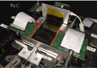
Lockheed Martin’s SPIDER (Segmented Planar Imaging Detector for Electro-optical Reconnaissance) concept trades bulky lenses and telescopes for a thin layer of hundreds or thousands of tiny lenses that feed photonic integrated circuits on silicon chips. These photonic circuits, developed by Professor Ben Yoo and his team at UC Davis’ Department of Electrical and Computer Engineering, combine the light from pairs of lenses to construct a digital image from the interference fringes caused by overlapping waves.
SPIDER eyes: Power in numbers
Interference fringes appear when waves coming from the same source through slightly different routes overlap. Think about ripples spreading in a pond. Where peaks or troughs coincide, they reinforce each other; where a peak meets a trough, they cancel out. When the waves originally came from the same source, the resulting interference patterns can yield information about their original state.
Large-scale astronomical interferometer arrays are already used to form ultra-high-resolution images of objects in space from optical and radio telescopes. The goal of SPIDER is to shrink that concept to a thin layer of thousands of lenses feeding silicon chips that can process photons.
Page 1 of 2
Share on:


Suggested Items
Inkjet Solder Mask ‘Has Arrived’
04/10/2024 | Pete Starkey, I-Connect007I was delighted to be invited to attend an interactive webinar entitled “Solder Mask Coating Made Easy with Additive Manufacturing,” hosted by SUSS MicroTec Netherlands in Eindhoven. The webinar was introduced and moderated by André Bodegom, managing director at Adeon Technologies, and the speakers were Mariana Van Dam, senior product manager PCB imaging solutions at AGFA in Belgium; Ashley Steers, sales manager at Electra Polymers in the UK; and Dr. Luca Gautero, product manager at SUSS MicroTec Netherlands.
NetVia Group Acquires Direct Imaging from Mivatek
04/09/2024 | Miva TechnologiesMiva Technologies is pleased to announce NetVia Group, Irving, TX has acquired a new Miva 2400NG Dual Tray Direct Imaging System with 30-micron capabilities for inner, outer and soldermask imaging.
Teledyne to Acquire Adimec
02/13/2024 | TeledyneTeledyne Technologies Incorporated announced that it has entered into an agreement to acquire Adimec Holding B.V. and its subsidiaries.
Real Time with... productronica 2023: MivaTek Global Advances Technology With High-res Imaging System
12/08/2023 | Real Time with...productronicaMivaTek's Brendan Hogan talks about how the company employs Digitally Adaptive Rasterization Technology (DART) in their high-res imaging equipment. He also shares how the blurred line between semiconductors and microelectronics is driving broader application of the imaging process.
Keysight Enables Validation of Arbe 4D Imaging Radar Chipset
11/30/2023 | Keysight Technologies, Inc.Keysight Technologies, Inc. announces that Arbe has selected the E8719A Radar Target Solution (RTS) to test the Arbe 4D imaging radar chipset for automotive applications.