


 The Government Circuit: Driving Resiliency and Economic Security on Both Sides of the Atlantic
 American Made Advocacy: Taking the Fight to Capitol Hill
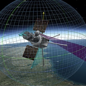
 Defense Speak Interpreted: SWaPing Nanosatellites for Defense Systems
Latent Short Circuit Failure in High-Rel PCBs due to Cleanliness of PCB Processes and Base Materials
August 11, 2015 | Stan HeltzelEstimated reading time: 2 minutes

Latent short circuit failures have been observed during testing of PCBs for power distribution of spacecraft of the European Space Agency. Root cause analysis indicates that foreign fibers may have contaminated the PCB laminate. These fibers can provide a pathway for electromigration if they bridge the clearance between nets of different potential in the presence of humidity attracted by the hygroscopic laminate resin. PCB manufacturers report poor yield caused by contamination embedded in laminate. Inspections show that fiber contamination is present on prepreg and etched innerlayers. Further fiber contamination may be attracted in the manufacturing environment due to static charging. The requirements for cleanliness that are specified for final PCBs are orders of magnitude more stringent than
those specified for base materials. This paper describes inspections performed on base materials, manufacturing processes and final PCBs. It describes test methods that detect reduced insulation caused by contamination and electromigration. Moreover, a proposal is presented specifying tightened requirements for a new class of base materials for the manufacture of high-reliability PCBs.
I. Introduction
Latent short circuit failures have been observed in PCBs during testing of power distribution units of spacecraft for the European Space Agency (ESA). Root cause analysis has been conducted under review of non-conformance review boards (NRB). Printed circuit board assemblies failed after prolonged functional testing in ambient laboratory environment or after thermal vacuum cycles. Due to the large amount of damage caused by the electrical overstress, it was not possible to obtain direct evidence of the failure. However, a working hypothesis has been developed indicating that fiber contamination may have caused a latent short circuit. This hypothesis was further substantiated by reports on contamination issues in base materials and by a test method that demonstrated the breach of insulation due to fiber contamination.
At the time of the observed failures at equipment level, PCB manufacturers reported poor cleanliness levels of base laminate materials, causing poor yield. It is not possible to screen in an efficient manner for contamination in copper-clad laminate, since visual inspection requires stripping of the copper. Several inspection methods show the lack of cleanliness of base materials, which is specified in IPC4101[8]. This paper identifies a major gap between the requirements specified on base materials and the requirements on manufactured PCBs and presents a proposal for a new class of cleaner base materials for the manufacture of high-rel PCBs.
Editor's Note: This article originally appeared in the August 2015 issue of The PCB Magazine.
Share on:


Suggested Items
Insulectro’s 'Storekeepers' Extend Their Welcome to Technology Village at IPC APEX EXPO
04/03/2024 | InsulectroInsulectro, the largest distributor of materials for use in the manufacture of PCBs and printed electronics, welcomes attendees to its TECHNOLOGY VILLAGE during this year’s IPC APEX EXPO at the Anaheim Convention Center, April 9-11, 2024.
ENNOVI Introduces a New Flexible Circuit Production Process for Low Voltage Connectivity in EV Battery Cell Contacting Systems
04/03/2024 | PRNewswireENNOVI, a mobility electrification solutions partner, introduces a more advanced and sustainable way of producing flexible circuits for low voltage signals in electric vehicle (EV) battery cell contacting systems.
Heavy Copper PCBs: Bridging the Gap Between Design and Fabrication, Part 1
04/01/2024 | Yash Sutariya, Saturn Electronics ServicesThey call me Sparky. This is due to my talent for getting shocked by a variety of voltages and because I cannot seem to keep my hands out of power control cabinets. While I do not have the time to throw the knife switch to the off position, that doesn’t stop me from sticking screwdrivers into the fuse boxes. In all honesty, I’m lucky to be alive. Fortunately, I also have a talent for building high-voltage heavy copper circuit boards. Since this is where I spend most of my time, I can guide you through some potential design for manufacturability (DFM) hazards you may encounter with heavy copper design.
Trouble in Your Tank: Supporting IC Substrates and Advanced Packaging, Part 5
03/19/2024 | Michael Carano -- Column: Trouble in Your TankDirect metallization systems based on conductive graphite or carbon dispersion are quickly gaining acceptance worldwide. Indeed, the environmental and productivity gains one can achieve with these processes are outstanding. In today’s highly competitive and litigious environment, direct metallization reduces costs associated with compliance, waste treatment, and legal issues related to chemical exposure. What makes these processes leaders in the direct metallization space?
AT&S Shines with Purest Copper on World Recycling Day
03/18/2024 | AT&SThe Styrian microelectronics specialist AT&S is taking World Recycling Day as an opportunity to review the progress that has been made in recent months at its sites around the world in terms of the efficient use of resources: