


 The Government Circuit: Driving Resiliency and Economic Security on Both Sides of the Atlantic
 American Made Advocacy: Taking the Fight to Capitol Hill
 Defense Speak Interpreted: SWaPing Nanosatellites for Defense Systems
Ventec, BizLink, Footprintku Announce Strategic Alliance
February 26, 2021 | VentecEstimated reading time: 1 minute
Ventec is pleased to announce that it has entered into a global strategic alliance with leading interconnect solutions provider, BizLink Holding Inc., and Footprintku Inc., an online EDA library and digital transformation services provider for electronic components. This alliance is formed to provide a solution that boosts product development process efficiency and shortens development and time-to-market.
BizLink has long been a supplier of key components to the IT industry, including connectors and cables. The company is experienced in new product introduction (NPI) as well as in system integration, manufacturing, and in assembly.
BizLink’s Chairman, Roger Liang, said, "For the design of electronic products, the trend is for thinner, lighter, and aesthetically pleasing products whilst maintaining functionality and compatibility. This has prompted the demand for rapid and frequent updates of components and product styles. The ability to quickly develop products to respond to market changes has become the key to success."
Ventec International’s Chairman, Tony Lau, pointed out, "What the market needs is a platform that integrates the advantages of upstream components, mid-section design, and back-end manufacturing. The creation of such a platform, we knew, would greatly help accelerate industrial innovation." Footprintku Inc.’s Chairman, YC Hwang, continued, "In response, we propose a cloud platform using the exclusive AI and digital transformation technology of Footprintku.com to integrate the resources of all three companies. The result is a one-stop service, making it possible for product developers to quickly and efficiently find the best components and quality suppliers for their product R&D and design change stages."
This alliance is built upon Footprintku’s cloud database for electronic components as well as BizLink’s solutions and Ventec International’s materials. It integrates the capabilities of new product introduction (NPI), design services (ODM), and manufacturing assembly (EMS). This alliance will reduce the cost of and time in searching for electronic components for product developers. Furthermore, it will accelerate product evolution and facilitate industrial innovation by connecting highly flexible and customized electronic industry supply chain partners.
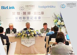
The alliance was officially announced at a press conference held at the Grand Hyatt Taipei on February 26, 2021.
Share on:


Suggested Items
Designer’s Notebook: What Designers Need to Know About Manufacturing, Part 2
04/24/2024 | Vern Solberg -- Column: Designer's NotebookThe printed circuit board (PCB) is the primary base element for providing the interconnect platform for mounting and electrically joining electronic components. When assessing PCB design complexity, first consider the component area and board area ratio. If the surface area for the component interface is restricted, it may justify adopting multilayer or multilayer sequential buildup (SBU) PCB fabrication to enable a more efficient sub-surface circuit interconnect.
Insulectro’s 'Storekeepers' Extend Their Welcome to Technology Village at IPC APEX EXPO
04/03/2024 | InsulectroInsulectro, the largest distributor of materials for use in the manufacture of PCBs and printed electronics, welcomes attendees to its TECHNOLOGY VILLAGE during this year’s IPC APEX EXPO at the Anaheim Convention Center, April 9-11, 2024.
ENNOVI Introduces a New Flexible Circuit Production Process for Low Voltage Connectivity in EV Battery Cell Contacting Systems
04/03/2024 | PRNewswireENNOVI, a mobility electrification solutions partner, introduces a more advanced and sustainable way of producing flexible circuits for low voltage signals in electric vehicle (EV) battery cell contacting systems.
Heavy Copper PCBs: Bridging the Gap Between Design and Fabrication, Part 1
04/01/2024 | Yash Sutariya, Saturn Electronics ServicesThey call me Sparky. This is due to my talent for getting shocked by a variety of voltages and because I cannot seem to keep my hands out of power control cabinets. While I do not have the time to throw the knife switch to the off position, that doesn’t stop me from sticking screwdrivers into the fuse boxes. In all honesty, I’m lucky to be alive. Fortunately, I also have a talent for building high-voltage heavy copper circuit boards. Since this is where I spend most of my time, I can guide you through some potential design for manufacturability (DFM) hazards you may encounter with heavy copper design.
Trouble in Your Tank: Supporting IC Substrates and Advanced Packaging, Part 5
03/19/2024 | Michael Carano -- Column: Trouble in Your TankDirect metallization systems based on conductive graphite or carbon dispersion are quickly gaining acceptance worldwide. Indeed, the environmental and productivity gains one can achieve with these processes are outstanding. In today’s highly competitive and litigious environment, direct metallization reduces costs associated with compliance, waste treatment, and legal issues related to chemical exposure. What makes these processes leaders in the direct metallization space?