


 The Government Circuit: Driving Resiliency and Economic Security on Both Sides of the Atlantic
 American Made Advocacy: Taking the Fight to Capitol Hill
 Defense Speak Interpreted: SWaPing Nanosatellites for Defense Systems
RBP Chemical Technology Announces the Release of ONYX™ Direct Metallization System for PCBs
March 11, 2020 | RBP Chemical TechnologyEstimated reading time: 1 minute
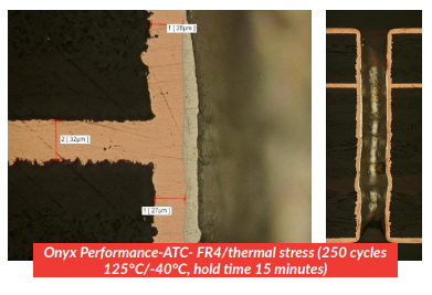
RBP’s ONYX™ is a Direct Metallization System for high reliability and complex printed circuit boards.
The RBP ONYX™ Direct Metallization Process is an integrated system based on a highly conductive form of finely dispersed graphite. Extensively tested and validated, the ONYX™ Process has proven to be versatile and cost effective. Currently the customer base using ONYX™ processes flex, rigid-flex, HDI and high aspect ratio multilayer printed circuit boards with ease and cost effectiveness when compared to conventional electroless copper. The ONYX™ process easily surpasses industry reliability standards including IST (interconnection stress test) and ATC (accelerated thermal cycling).
ONYX™ Direct Metallization System Highlights
The ONYX™ Direct Metallization System is a versatile process and is used in horizontal conveyorized equipment or in vertical immersion mode. Fabricators are able to process a vast array of resin materials including PTFE, polyimide, BT, flex, and basically all epoxy-based resin systems on the market today.
This process is an alternative to electroless copper deposition and provides several significant benefits to the fabricator:
- Less expensive than conventional electroless copper
- Smaller equipment footprint compared to electroless copper
- Greatly reduced water consumption, 4?6 gallons/minute, compared to conventional electroless copper, 26?30 gallons per minute
- ONYX™ contains no chelator as opposed to electroless copper—simplifying waste treatment
About RBP
RBP Chemical Technology is a leading supplier of proprietary chemicals for printed circuit fabrication and semiconductor test applications. RBP’s chemical formulas are tailored to meet the precise needs and requirements for advanced circuit boards, primarily in aerospace, medical and military applications. Headquartered in Milwaukee, Wisconsin and expanding globally, RBP is certified to ISO 9001:2015 and is the Intelligent Choice for the electronics industry.
Share on:


Suggested Items
Designer’s Notebook: What Designers Need to Know About Manufacturing, Part 2
04/24/2024 | Vern Solberg -- Column: Designer's NotebookThe printed circuit board (PCB) is the primary base element for providing the interconnect platform for mounting and electrically joining electronic components. When assessing PCB design complexity, first consider the component area and board area ratio. If the surface area for the component interface is restricted, it may justify adopting multilayer or multilayer sequential buildup (SBU) PCB fabrication to enable a more efficient sub-surface circuit interconnect.
Insulectro’s 'Storekeepers' Extend Their Welcome to Technology Village at IPC APEX EXPO
04/03/2024 | InsulectroInsulectro, the largest distributor of materials for use in the manufacture of PCBs and printed electronics, welcomes attendees to its TECHNOLOGY VILLAGE during this year’s IPC APEX EXPO at the Anaheim Convention Center, April 9-11, 2024.
ENNOVI Introduces a New Flexible Circuit Production Process for Low Voltage Connectivity in EV Battery Cell Contacting Systems
04/03/2024 | PRNewswireENNOVI, a mobility electrification solutions partner, introduces a more advanced and sustainable way of producing flexible circuits for low voltage signals in electric vehicle (EV) battery cell contacting systems.
Heavy Copper PCBs: Bridging the Gap Between Design and Fabrication, Part 1
04/01/2024 | Yash Sutariya, Saturn Electronics ServicesThey call me Sparky. This is due to my talent for getting shocked by a variety of voltages and because I cannot seem to keep my hands out of power control cabinets. While I do not have the time to throw the knife switch to the off position, that doesn’t stop me from sticking screwdrivers into the fuse boxes. In all honesty, I’m lucky to be alive. Fortunately, I also have a talent for building high-voltage heavy copper circuit boards. Since this is where I spend most of my time, I can guide you through some potential design for manufacturability (DFM) hazards you may encounter with heavy copper design.
Trouble in Your Tank: Supporting IC Substrates and Advanced Packaging, Part 5
03/19/2024 | Michael Carano -- Column: Trouble in Your TankDirect metallization systems based on conductive graphite or carbon dispersion are quickly gaining acceptance worldwide. Indeed, the environmental and productivity gains one can achieve with these processes are outstanding. In today’s highly competitive and litigious environment, direct metallization reduces costs associated with compliance, waste treatment, and legal issues related to chemical exposure. What makes these processes leaders in the direct metallization space?