


 The Government Circuit: Driving Resiliency and Economic Security on Both Sides of the Atlantic
 American Made Advocacy: Taking the Fight to Capitol Hill
 Defense Speak Interpreted: SWaPing Nanosatellites for Defense Systems
Graphene Key to Two-dimensional Semiconductor with Extraordinary Properties
August 30, 2016 | Pennsylvania State UniversityEstimated reading time: 3 minutes
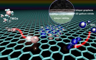
A newly discovered method for making two-dimensional materials could lead to new and extraordinary properties, particularly in a class of materials called nitrides, say the Penn State materials scientists who discovered the process. This first-ever growth of two-dimensional gallium nitride using graphene encapsulation could lead to applications in deep ultraviolet lasers, next-generation electronics and sensors.
"These experimental results open up new avenues of research in 2D materials," says Joshua Robinson, associate professor of materials science and engineering. "This work focuses on making 2D gallium nitride, which has never been done before."
Gallium nitride in its three-dimensional form is known to be a wide-bandgap semiconductor. Wide-bandgap semiconductors are important for high frequency, high power applications. When grown in its two-dimensional form, gallium nitride transforms from a wide-bandgap material to an ultrawide-bandgap material, effectively tripling the energy spectrum it can operate in, including the whole ultraviolet, visible and infrared spectrum. This work will have a particular impact on electro-optic devices that manipulate and transmit light.
"This is a new way of thinking about synthesizing 2D materials," said Zak Al Balushi, a Ph.D. candidate coadvised by Robinson and Joan Redwing, professor of materials science and engineering and electrical engineering. Al Balushi is lead author on a paper appearing online today (Aug.29) in the journal Nature Materials titled "Two-Dimensional Gallium Nitride Realized via Graphene Encapsulation."
"We have this palette of naturally occurring 2D materials," he continued. "But to expand beyond this, we have to synthesize materials that do not exist in nature. Typically, new material systems are highly unstable. But our growth method, called Migration Enhanced Encapsulated Growth (MEEG), uses a layer of graphene to assist the growth and stabilize a robust structure of 2D gallium nitride."
The graphene is grown on a substrate of silicon carbide, which is a technologically important substrate used widely in industry for LEDs, radar and telecommunications. When heated, the silicon on the surface decomposes and leaves a carbon-rich surface that can reconstruct into graphene. The advantage of producing the graphene in this way is that the interface where the two materials meet is perfectly smooth.
Robinson believes that in the case of two-dimensional gallium nitride, the addition of a layer of graphene makes all the difference. Graphene, a one-atom-thick layer of carbon atoms, is known for its remarkable electronic properties and strength.
"It's the key," Robinson says. "If you try to grow these materials the traditional way, on silicon carbide, you normally just form islands. It doesn't grow in nice layers on the silicon carbide."
When gallium atoms are added to the mix, they migrate through the graphene and form the middle layer of a sandwich, with graphene floating on top. When nitrogen atoms are added, a chemical reaction takes place that turns the gallium and nitrogen into gallium nitride.
"The MEEG process not only produces ultra-thin sheets of gallium nitride but also changes the crystal structure of the material, which may lead to entirely new applications in electronics and optoelectronics," said Redwing.
Additional coauthors include Ke Wang, Rafael Vila, Sarah Eichfield, Yu-Chuan Lin and Shruti Subramanian of Penn State, Ram Krishna Ghosh and Suman Datta of Notre Dame, Joshua Caldwell, U.S. Naval Research Laboratory, Xiaoye Qin and Robert Wallace The University of Texas at Dallas and Dennis Paul, Physical Electronics USA.
The Asahi Glass Co., Ltd, Japan, and the U.S. National Science Foundation provided funding for this project. The NSF Materials Science and Engineering Center at Penn State provided funding for Al Balushi. Other funding was provided by the Alfred P. Sloan Foundation, the Penn State Materials Characterization Laboratory and the Center for Low Energy Systems Technology (LEAST), funded by the Semiconductor Research Corporation and DARPA.
Share on:


Suggested Items
LQDX Divests Aluminum Soldering Business - Mina™ - to Taiyo America Inc.
05/02/2024 | PRNewswireLQDX, formerly known as Averatek Corp., developer of high-performance materials for advanced semiconductor manufacturing, today announced that it has divested its aluminum soldering business – known as MinaTM – to Taiyo America Inc., a global market leader in advanced electronic materials.
Indium Corporation Expert to Present on Pb-Free Solder for Die-Attach in Discrete Power Applications
04/30/2024 | Indium CorporationIndium Corporation Product Manager – Semiconductor Dean Payne will present at the Advanced Packaging for Power Electronics conference, hosted by IMAPS, held May 8-9 in Woburn, Massachusetts, USA.
Real Time with... IPC APEX EXPO 2024: Adhesive Materials and Equipment Update with Dymax
05/01/2024 | Real Time with...IPC APEX EXPOVirginia Hogan, global business development manager at Dymax, discusses adhesive materials, dispensing and curing equipment, a new, high-reliability conformal coating, and various materials and dispensing methods.
Real Time with... IPC APEX EXPO 2024: Sustainability in the Industry
04/26/2024 | Real Time with...IPC APEX EXPOGuest Editor Henry Crandall and Chris Nash of Indium Corporation discuss the company's 90th anniversary and its focus on sustainability. They focus on the benefits of sustainable materials, their compatibility, and value propositions. The conversation also highlights how Durafuse LT technology's role in reducing reflow temperatures is leading to significant cost and energy savings. Nash also touches on downstream sustainability efforts such as using recycled materials for packaging.
SMC Korea 2024 to Highlight Semiconductor Materials Trends and Innovations on Industry’s Path to $1 Trillion
04/24/2024 | SEMIWith Korea a major consumer of semiconductor materials and advanced materials a key driver of innovation on the industry’s path to $1 trillion, industry leaders and experts will gather at SMC (Strategic Materials Conference) Korea 2024 on May 29 at the Suwon Convention Center in Gyeonggi-do, South Korea to provide insights into the latest materials developments and trends. Registration is open.