


 The Government Circuit: Driving Resiliency and Economic Security on Both Sides of the Atlantic
 American Made Advocacy: Taking the Fight to Capitol Hill
 Defense Speak Interpreted: SWaPing Nanosatellites for Defense Systems
NASA Investigates 3-D Printing for Building Densely Populated Electronic Assemblies
April 26, 2016 | NASAEstimated reading time: 2 minutes
As detector assemblies get smaller and denser — packed with electronic components that all must be electrically connected to sense and read out signals — it’s becoming increasingly more challenging to design and manufacture these all-important instrument devices.
A team of NASA technologists at the Goddard Space Flight Center in Greenbelt, Maryland, however, has begun investigating the use of a technique called aerosol jet printing or direct-write manufacturing to produce new detector assemblies that are not possible with traditional assembly processes.
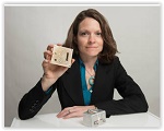
“If we succeed, aerosol jet technology could define a whole new way to create dense electronic board assemblies and potentially improve the performance and consistency of electronic assemblies,” explained Goddard technologist Beth Paquette, who is leading the R&D effort that began last fiscal year. Furthermore, aerosol jet printing promises to slash the time it takes to manufacture circuit boards, from a month to a day or two, she added.
Important Distinction
As with other 3-D printing techniques, aerosol jet manufacturing builds components by depositing materials layer-by-layer following a computer-aided design, or CAD, drawing. However, jet aerosol printing offers an important difference.
Instead of melting and fusing plastic powder or some other material in precise locations, as in the case of many 3-D printers, aerosol jet printing uses a carrier gas and printer heads to deposit a fine aerosol of metal particles, including silver, gold, platinum, or aluminum, onto a surface. Aerosol jet printers also can deposit polymers or other insulators and can even print carbon nanotubes, cylindrically shaped carbon molecules that have novel properties useful in nanotechnology, electronics, and optics.
“It can print around bends, on spheres or on something flat, or on a flexible surface, which then can be flexed into the shape you want,” she said.
These attributes make the technology ideal for detector assemblies, particularly those that need to be shaped differently or are very small, yet dense because of the large number of tiny components that must be electrically wired or linked together on a circuit board — an inescapable reality as instruments get smaller and smaller.
“We can make these wires microns in width,” Paquette said. “These lines are very small, down to 10 microns wide. These sizes aren’t possible using traditional circuit board manufacturing processes.” (By way of comparison, the average human hair measures between 17 and 191 microns in width.)
Page 1 of 2
Share on:


Suggested Items
Warm Windows and Streamlined Skin Patches – IDTechEx Explores Flexible and Printed Electronics
04/26/2024 | IDTechExFlexible and printed electronics can be integrated into cars and homes to create modern aesthetics that are beneficial and easy to use. From luminous car controls to food labels that communicate the quality of food, the uses of this technology are endless and can upgrade many areas of everyday life.
iNEMI Packaging Tech Topic Series: Role of EDA in Advanced Semiconductor Packaging
04/26/2024 | iNEMIAdvanced semiconductor packaging with heterogenous integration has made on-package integration of multiple chips a crucial part of finding alternatives to transistor scaling. Historically, EDA tools for front-end and back-end design have evolved separately; however, design complexity and the increased number of die-to-die or die-to-substrate interconnections has led to the need for EDA tools that can support integration of overall design planning, implementation, and system analysis in a single cockpit.
Koh Young Showcases Award-winning Inspection Solutions at SMTconnect with SmartRep in Hall 4A.225
04/25/2024 | Koh Young TechnologyKoh Young Technology, the industry leader in True 3D measurement-based inspection solutions, will showcase an array of award-winning inspection and measurement solutions at SMTconnect alongside its sales partner, SmartRep, in booth 4A.225 at NürnbergMesse from June 11-13, 2023. The following offers a glimpse into what Koh Young will present at the tradeshow:
Real Time with… IPC APEX EXPO 2024: Plasmatreat: Innovative Surface Preparation Solutions
04/25/2024 | Real Time with...IPC APEX EXPOIn this interview, Editor Nolan Johnson speaks with Hardev Grewal, CEO and president of Plasmatreat, a developer of atmospheric plasma solutions. Plasmatreat uses clean compressed air and electricity to create plasma, offering environmentally friendly methods for surface preparation. Their technology measures plasma density for process optimization and can remove organic micro-contamination. Nolan and Hardev also discuss REDOX-Tool, a new technology for removing metal oxides.
Nanotechnology Market to Surpass $53.51 Billion by 2031
04/25/2024 | PRNewswireSkyQuest projects that the nanotechnology market will attain a value of USD 53.51 billion by 2031, with a CAGR of 36.4% over the forecast period (2024-2031).