


 The Government Circuit: Driving Resiliency and Economic Security on Both Sides of the Atlantic
 American Made Advocacy: Taking the Fight to Capitol Hill
 Defense Speak Interpreted: SWaPing Nanosatellites for Defense Systems
New Chips Ease Operations In Electromagnetic Environs
January 12, 2016 | DARPAEstimated reading time: 2 minutes
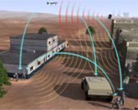
Competition for scarce electromagnetic (EM) spectrum is increasing, driven by a growing military and civilian demand for connected devices. As the spectrum becomes more congested, the Department of Defense (DoD) will need better tools for managing the EM environment and for avoiding interference from competing signals. One recent DARPA-funded advance, an exceptionally high-speed analog-to-digital converter (ADC), represents a major step forward. The ADC could help ensure the uninterrupted operation of spectrum-dependent military capabilities, including communications and radar, in contested EM environments. The advance was enabled by 32 nm silicon-on-insulator (SOI) semiconductor technologies available through DARPA’s ongoing partnership with GlobalFoundries, a manufacturer of highly-advanced semiconductor chips.
The EM spectrum, whose component energy waves include trillionth-of-a-meter-wavelength gamma rays to multi-kilometer-wavelength radio waves, is an inherently physical phenomenon. ADCs convert physical data—that is, analog data—on the spectrum into numbers that a digital computer can analyze and manipulate, an important capability for understanding and adapting to dynamic EM environments.
Today’s ADCs, however, only process data within a limited portion of the spectrum at a given time. As a result, they can temporarily overlook critical information about radar, jamming, communications, and other potentially problematic EM signals. DARPA’s Arrays at Commercial Timescales (ACT) program addressed this challenge by supporting the development of an ADC with a processing speed nearly ten times that of commercially available, state-of-the-art alternatives. By leveraging this increased speed, the resulting ADC can analyze data from across a much wider spectrum range, allowing DoD systems to better operate in congested spectrum bands and to more rapidly react to spectrum-based threats.
How fast is fast? The new ADC samples and digitizes spectrum signals at a rate of over 60 billion times per second (60 GigaSamples/sec). That’s fast enough to directly detect and analyze any signal at 30 GHz or below—a range that encompasses the vast majority of operating frequencies of interest. Whereas scanning through these frequencies today requires costly application-specific hardware with long development cycles, the new ADC can provide a “one-stop shop” for processing radar, communications and electronic warfare signals.
Page 1 of 2
Share on:


Suggested Items
iNEMI Names Grace O'Malley CTO
05/02/2024 | iNEMIThe Board of Directors of the International Electronics Manufacturing Initiative (iNEMI) has named Grace O'Malley Chief Technical Officer (CTO).
Dubai Launches Global Blueprint for Artificial Intelligence
05/02/2024 | BUSINESS WIREDubai has launched a blueprint for Artificial Intelligence (AI), a yearly plan that will focus on harnessing the technology’s potential to improve quality of life around the world.
NextFlex Convenes the Hybrid Electronics Community at Binghamton University
05/01/2024 | NextFlexBinghamton University hosted the NextFlex hybrid electronics community on April 18 for a day of expert presentations, breakout sessions on technology and manufacturing topics, and networking.
IDTechEx Report on Quantum Technology: Nano-scale Physics for Massive Market Impact
04/30/2024 | PRNewswireThe quantum technology market leverages nano-scale physics to create revolutionary new devices for computing, sensing, and communications. Across the industry, quantum technology offers a paradigm shift in performance compared with incumbent solutions.
TSMC Certifies Ansys Multiphysics Platforms, Enabling Next-Gen AI and HPC Chips
04/30/2024 | PRNewswireAnsys announced the certification of its power integrity platforms for TSMC's N2 technology full production release. Both Ansys RedHawk-SC and Ansys Totem are certified for power integrity signoff on the N2 process, delivering significant speed and power advantages for high performance computing, mobile chips, and 3D-IC designs.