


 The Government Circuit: Driving Resiliency and Economic Security on Both Sides of the Atlantic
 American Made Advocacy: Taking the Fight to Capitol Hill
 Defense Speak Interpreted: SWaPing Nanosatellites for Defense Systems
NRL Takes LEAP in NextGen Materials Design
July 28, 2015 | U.S. Naval Research LaboratoryEstimated reading time: 2 minutes
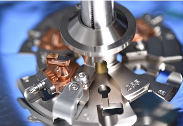
The U.S. Naval Research Laboratory (NRL), Materials Science and Technology Division, has taken delivery of a state-of-the-art Cameca 4000X Si Local Electrode Atom Probe (LEAP), a high performance microscope that provides precise atom-by-atom dissection of a material volume, enabling true three-dimensional (3D) atomic-scale reconstructions of material microstructures.
Local Electrode Atom Probe (LEAP) microscopeThe U.S. Naval Research Laboratory, Washington, D.C., has taken delivery of the only Local Electrode Atom Probe (LEAP) microscope in use in the U.S. Department of Defense (DoD). Researchers at the laboratory's Materials Science and Technology Division will utilize the atom probe to analyze materials at the atomic level for optimizing new, next-generation alloys and semiconducting materials.
"Exact knowledge of where individual atoms are in a material is of tremendous benefit when engineering new materials," said Keith Knipling, NRL Materials Science and Technology Division. "We expect the LEAP to greatly enhance our capability to develop new materials, including the next generation of structural alloys for stronger ship hulls and more advanced turbine engines, new electronic materials for tomorrow's faster integrated circuits, and advanced solar cell and battery materials with improved power and energy efficiency."
The LEAP works using the principle of field evaporation, whereby a strong electric field applied to a needle-like specimen is sufficient to cause removal of atoms by ionization. Atom evaporation is triggered either by a voltage or laser pulse applied to the sample. The resulting ions are accelerated away from the specimen and identified chemically by time-of-flight mass spectrometry and their positions are deduced from the coordinates of ion impacts on a position-sensitive detector. By repeating this sequence, the atoms are progressively removed from the tip, and a 3D image of the material can be reconstructed at the atomic scale.
"Mapping the location of each chemical species in a material microstructure enables an unprecedented understanding of the true effects of alloying and material synthesis, which is essential for truly optimizing the properties of any material. We expect the LEAP to deliver new atomic-scale perspective and insights into a wide range of materials science investigations. For example, researchers at NRL are developing semiconductor materials with very dilute levels of added 'dopant' atoms for the purpose of tailoring their electrical properties," Knipling adds. "These doped materials form the building blocks of nearly all semiconductor electronic devices such as diodes, transistors, solar cells, LEDs, and integrated circuits. Most analytical techniques are incapable of measuring these small concentration levels, much less where the dopants segregate within the microstructure. With the LEAP, researchers can now answer these questions."
Worldwide, there are only a handful of LEAP microscopes in use. NRL Materials Science and Technology Division possesses the only one in use by the U.S. Department of Defense (DoD).
Share on:


Suggested Items
Warm Windows and Streamlined Skin Patches – IDTechEx Explores Flexible and Printed Electronics
04/26/2024 | IDTechExFlexible and printed electronics can be integrated into cars and homes to create modern aesthetics that are beneficial and easy to use. From luminous car controls to food labels that communicate the quality of food, the uses of this technology are endless and can upgrade many areas of everyday life.
iNEMI Packaging Tech Topic Series: Role of EDA in Advanced Semiconductor Packaging
04/26/2024 | iNEMIAdvanced semiconductor packaging with heterogenous integration has made on-package integration of multiple chips a crucial part of finding alternatives to transistor scaling. Historically, EDA tools for front-end and back-end design have evolved separately; however, design complexity and the increased number of die-to-die or die-to-substrate interconnections has led to the need for EDA tools that can support integration of overall design planning, implementation, and system analysis in a single cockpit.
Koh Young Showcases Award-winning Inspection Solutions at SMTconnect with SmartRep in Hall 4A.225
04/25/2024 | Koh Young TechnologyKoh Young Technology, the industry leader in True 3D measurement-based inspection solutions, will showcase an array of award-winning inspection and measurement solutions at SMTconnect alongside its sales partner, SmartRep, in booth 4A.225 at NürnbergMesse from June 11-13, 2023. The following offers a glimpse into what Koh Young will present at the tradeshow:
Real Time with… IPC APEX EXPO 2024: Plasmatreat: Innovative Surface Preparation Solutions
04/25/2024 | Real Time with...IPC APEX EXPOIn this interview, Editor Nolan Johnson speaks with Hardev Grewal, CEO and president of Plasmatreat, a developer of atmospheric plasma solutions. Plasmatreat uses clean compressed air and electricity to create plasma, offering environmentally friendly methods for surface preparation. Their technology measures plasma density for process optimization and can remove organic micro-contamination. Nolan and Hardev also discuss REDOX-Tool, a new technology for removing metal oxides.
Nanotechnology Market to Surpass $53.51 Billion by 2031
04/25/2024 | PRNewswireSkyQuest projects that the nanotechnology market will attain a value of USD 53.51 billion by 2031, with a CAGR of 36.4% over the forecast period (2024-2031).