


 The Government Circuit: Driving Resiliency and Economic Security on Both Sides of the Atlantic
 American Made Advocacy: Taking the Fight to Capitol Hill
 Defense Speak Interpreted: SWaPing Nanosatellites for Defense Systems
Enabling Extreme New Designs for Optics and Imagers
August 22, 2016 | DARPAEstimated reading time: 2 minutes
Developers of imaging systems have long been beholden to certain rules of optics designs so well established and seemingly immutable as to be treated as virtual “laws” of physics. One widely considered pillar of optical design, for example, is that imaging systems must be built from a series of complex and precisely manufactured optical elements arranged linearly. The result of such assumptions is that certain high-performance imagery devices inevitably end up being large and heavy, composed of dozens or more optical elements. DARPA’s EXTREME Optics and Imaging (EXTREME) program aims to break from that well-worn paradigm by introducing engineered optical materials (EnMats) and associated design tools for creating innovative optical systems with improved performance, new functionality, and drastically reduced size and weight.
A special notice was issued today announcing the EXTREME Proposers Day on September 1, 2016, via webcast to familiarize potential proposers with the goals of the program. A Broad Agency Announcement solicitation is also expected to be posted on DARPA’s FedBizOpps page in the near future.
“We’ve seen significant technical advances in recent years in the communities of optical system design, materials science and fabrication, and multiscale modeling and optimization,” said Predrag Milojkovic, DARPA program manager. “EXTREME seeks to capitalize on this momentum by uniting these separate communities to revolutionize optics and imaging as we know it.”
To achieve its goal, EXTREME is focused on developing new EnMats—both two-dimensional metasurfaces as well as 3-D volumetric optics and holograms—that manipulate light in ways beyond classical rules of reflection and refraction. EXTREME also will address multiscale modelling to enable design and optimization of EnMats across vastly different scales, from nanometer to centimeter, for example.
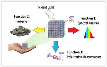
The program aims to demonstrate an optical system with engineered surfaces where control of light propagation is decoupled from a specific geometric shape and can be tuned. EXTREME also seeks to demonstrate a volumetric optical element the size of a sugar cube or larger that can perform a multitude of functions simultaneously in visual and infrared (IR) bands, such as imaging, spectrum analysis, and polarization measurements, among others.
If successful, EXTREME could introduce a new era in optics and imagers for national defense. EXTREME optical components would be lighter and smaller, enabling miniaturization of imaging systems for intelligence, surveillance, and reconnaissance (ISR) applications. The multifunctional nature of these devices could offer improvements in a wide variety of imaging systems by reducing size and weight without compromising performance for systems as diverse as night vision goggles, hyperspectral imagers, and IR search and track systems.
DARPA anticipates that reaching the objectives of the EXTREME program will require formation of cross-cutting teams bringing together expertise from disparate communities and fields, including but not limited to engineered material design and fabrication, multiscale modeling/simulation/optimization, and optical system design. Details on the upcoming Proposers Day are available here.
Share on:


Suggested Items
Real Time with... IPC APEX EXPO 2024: Exploring IPC's PCB Design Courses with Kris Moyer
04/18/2024 | Real Time with...IPC APEX EXPOGuest Editor Kelly Dack and IPC instructor Kris Moyer discuss IPC's PCB design training and education offerings. They delve into course topics such as design fundamentals, mil/aero, rigid-flex, RF design, and advanced design concepts. They also highlight material selection for high-speed design, thermal management, and dissipation techniques. The interview wraps up with details about how to access these courses online.
Cadence Unveils Palladium Z3 and Protium X3 Systems
04/18/2024 | Cadence Design SystemsThe Palladium Z3 and Protium X3 systems offer increased capacity, and scale from job sizes of 16 million gates up to 48 billion gates, so the largest SoCs can be tested as a whole rather than just partial models, ensuring proper functionality and performance.
Signal Integrity Expert Donald Telian to Teach 'Signal Integrity, In Practice' Masterclass Globally
04/17/2024 | PRLOGDonald Telian and The EEcosystem announce the global tour of "Signal Integrity, In Practice," a groundbreaking LIVE masterclass designed to equip hardware engineers with essential skills for solving Signal Integrity (SI) challenges in today's fast-paced technological landscape.
On the Line With... Podcast Talks With Cadence Expert on Manufacturing
04/18/2024 | I-Connect007In “PCB 3.0: A New Design Methodology: Manufacturing” Patrick Davis returns to the podcast to talk about design rules. As design considerations become more and more complex, so, too, do the rulesets designers must abide by.
Designing Electronics for High Thermal Loads
04/16/2024 | Akber Roy, Rush PCB Inc.Developing proactive thermal management strategies is important in the early stages of the PCB design cycle to minimize costly redesign iterations. Here, I delve into key aspects of electronic design that hold particular relevance for managing heat in electronic systems. Each of these considerations plays a pivotal role in enhancing the reliability and performance of the overall system.