


 The Government Circuit: Driving Resiliency and Economic Security on Both Sides of the Atlantic
 American Made Advocacy: Taking the Fight to Capitol Hill
 Defense Speak Interpreted: SWaPing Nanosatellites for Defense Systems
EIPC Summer Conference 2016, Day 2: Strategies to Maintain Profitability in the European PCB Industry
June 21, 2016 | Pete Starkey, I-Connect007Estimated reading time: 23 minutes
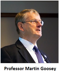
Delegates awoke to a wet and gloomy Scottish morning on the second day of the EIPC Summer Conference 2016. One or two who maybe overindulged in the whisky on the previous evening had some difficulty in finding time for breakfast before commencement of the conference proceedings, but the atmosphere in the meeting room was a lot brighter than the weather outside, as Professor Martin Goosey introduced the day’s programme, which began with a session of four presentations on the theme of future technology in components, materials and processes.
Title of the first paper was “Consistent miniaturisation, from conventional assembly to high-performance device embedding,” and because Michael Weinhold had to attend a family funeral, Alun Morgan stood in at short notice to deliver his presentation.
Weinhold commented that increased performance and functionality, as well as cost reduction, were the key drivers in electronic device manufacturing, and although different market segments had different needs, they shared the fundamental requirements of predicted product life expectancy and of meeting international material regulations and manufacturing standards. Moreover, repair of electronics devices in the field was now considered a no-go option. How would the European electronics industry realise these requirements, and how would the global consumer electronics market impact different market sectors? Key markets in Europe were military, avionics, space, medical, industrial and automotive, and each needed to be serviced by a specific supply chain. He set out discuss how PCB fabricators, EMS companies and OEMs could redirect their efforts to manufacture high-performing PCBs at the expected quality and cost whilst still achieving realistic profitability.
Weinhold had just returned from the JPCA show in Tokyo, where he had seen many examples of state-of-the-art technology, including mechanical drilling of 30 micron holes, with coated drill-bits for highly-filled laminates, six-layer multilayers on IMS materials for high thermal dissipation requirements, advances in all-electronic PCB-based 76GHz long-distance radar for automotive applications, drones operated from smart-phones, and an increasing number of modules and PCBs with embedded components.
Discussing possibilities for adding value to the PCB manufacturing process, Weinhold noted that PCB fabrication technology was dominated by Asia, and that bare PCBs represented only between 4% and 10% of the value of assembled boards. Against this background, he believed that European PCB fabricators had growth opportunities in new product developments with embedded devices.
Asked Weinhold, “What would change over coming years?” He believed that wireless interconnection interfaces would drive the development of new products, especially in the context of the Internet of Things, and that chips would be provided with wireless communication interphases, with an impact on connectors and assembly technology. Power electronics and applications handling voltages higher that 500V would have a significant effect on design and manufacturing of PCBs and assemblies, and new high-voltage test methods would be needed to meet operational life expectation of the industry and the end-user. Comparative tracking index would be an important parameter in new product developments. High-frequency PCBs would be required for faster data transfer in automotive, military, aerospace, avionics and medical electronics, as well as in high-speed networks: local, urban and global, and materials and fabrication processes would need to be adapted accordingly.
How would these changes affect the PCB fabricator? Component development would continue to drive miniaturization, and miniaturisation would drive the demand for cost reduction. The fabricator would need to achieve high yields on HDI and microvia product, and would need engineering expertise along the total process from design, through fabrication, assembly and testing. Product development could continue to be done in Europe and, provided companies understood market trends and needs, there could be many new R&D and product-development jobs. Having partners in low-cost countries would enable profits to be made on repeat orders and mass production. The essence of Weinhold’s message was “Understand your competence and positioning, find the right partners, build on the strength of your company and sell what you have!”
How many valuable PCBs are scrapped in process for shorts and opens caused by resist breakdown in plating and etching processes? The days when such defects could be repaired by knife-and-fork methods are now far behind us. For some time, Orbotech have offered automated optical repair systems for short circuits—using laser techniques to ablate unwanted copper, but what about the repair of open circuits by deposition of copper? It appeared from Alfred Kaiserman’s presentation that a solution is now available. Preferring not to use the term “repair” because of historical negative connotations, he described a laser-based “3D shaping” system, recently introduced by Orbotech under the name Precise™ 800.
He stated that the system automated the shaping process by way of two proprietary technologies: 3D Shaping (3DS) Technology™ and Closed Loop Shaping (CLS) Technology™. The 3DS™ additive technique was based on a series of processes, including 3D defect analysis, 3D laser shaping and 3D visualization. By comparing the shape of the defect to real-time CAM data and simultaneously conducting 3D analysis, 3DS™ automatically identified where copper needed to be added. It then guided a laser to a proprietary metal carrier from which copper was deposited in a series of thin layers to build up an exact 3D replica of the missing conductor, by a process of laser-induced forward transfer. The results could be confirmed immediately by 3D visualization. Kaiserman illustrated the operation with a video simulation. Conductors restored by this technique had been exhaustively tested to industry reliability standards, and there was a high level of confidence in their integrity. The subtractive function, CLS™, used image analysis algorithms to make real-time comparisons between the actual image and CAM data in order to detect the precise location of shorts and opens. It then intelligently guided the laser to accurately ablate excess copper. The system was clearly capable of significantly increasing yield and offered a rapid return on investment.Page 1 of 5
Share on:


Suggested Items
AIM to Highlight NC259FPA Ultrafine No Clean Solder Paste at SMTA Wisconsin Expo & Tech Forum
04/18/2024 | AIMAIM Solder, a leading global manufacturer of solder assembly materials for the electronics industry, is pleased to announce its participation in the upcoming SMTA Wisconsin Expo & Tech Forum taking place on May 7 at the Four Points by Sheraton | Milwaukee Airport, in Milwaukee, Wisconsin.
Hentec/RPS Publishes an Essential Guide to Selective Soldering Processing Tech Paper
04/17/2024 | Hentec Industries/RPS AutomationHentec Industries/RPS Automation, a leading manufacturer of selective soldering, lead tinning and solderability test equipment, announces that it has published a technical paper describing the critical process parameters that need to be optimized to ensure optimal results and guarantee the utmost in end-product quality.
Empowering Electronics Assembly: Introducing ALPHA Innolot MXE Alloy
04/16/2024 | MacDermid Alpha Electronics SolutionsIn the rapidly evolving electronics industry, where innovation drives progress, MacDermid Alpha Electronics Solutions is committed to setting a new standard. Today, we are pleased to introduce ALPHA Innolot MXE, a revolutionary alloy meticulously engineered to address the critical needs of enhanced reliability and performance in modern electronic assemblies.
New Book on Low-temperature Soldering Now Available
04/17/2024 | I-Connect007I-Connect007 is pleased to announce that The Printed Circuit Assembler’s Guide to… Low-temperature Soldering, Vol. 2, by subject matter experts at MacDermid Alpha Electronics Solutions, is now available for download.
Inkjet Solder Mask ‘Has Arrived’
04/10/2024 | Pete Starkey, I-Connect007I was delighted to be invited to attend an interactive webinar entitled “Solder Mask Coating Made Easy with Additive Manufacturing,” hosted by SUSS MicroTec Netherlands in Eindhoven. The webinar was introduced and moderated by André Bodegom, managing director at Adeon Technologies, and the speakers were Mariana Van Dam, senior product manager PCB imaging solutions at AGFA in Belgium; Ashley Steers, sales manager at Electra Polymers in the UK; and Dr. Luca Gautero, product manager at SUSS MicroTec Netherlands.