


 The Government Circuit: Driving Resiliency and Economic Security on Both Sides of the Atlantic
 American Made Advocacy: Taking the Fight to Capitol Hill
 Defense Speak Interpreted: SWaPing Nanosatellites for Defense Systems
300 W Adapter Reference Design from GaN Systems and ON Semiconductor Highlights GaN Innovation
December 20, 2019 | GaN SystemsEstimated reading time: 1 minute
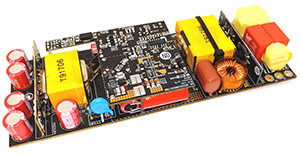
GaN Systems, the global leader in GaN (gallium nitride) power semiconductors and ON Semiconductor, a world-leading supplier of power semiconductor ICs, today announced the availability of the world’s highest power density 300 watt AC Adapter Reference Design using GaN Systems’ 650 V, 15 A GaN E-HEMTs and multiple award-winning ON Semiconductor Controller and Driver ICs: NCP51820, NCP13992, NCP1616, and NCP4306.
This complete system reference design is highly versatile and low cost, allowing designers to easily develop and bring to market ultra-high power density adapters for various applications in HDTV power supplies, gaming notebook and console adapters as well as ultra-small power supplies for industrial and medical devices.
The kit and application note provide detailed technical information including schematic, PCB layout, and BOM (bill of material) files, and EMI and efficiency data. The kit hardware has complete PFC, LLC, and secondary stages, and features a high-efficiency synchronous PFC which meets CoC T2 benchmark, a highly-versatile low-cost 2-Layer design, and universal input with 19 V Output at 340 W peak. System designers using this GaN-based reference design can reach power densities up to 32 watts per cubic inch.
“Fast-switching GaN works effectively with our advanced controller and drivers to optimize system designs for high power density, removing design barriers and enabling designers to take advantage of the numerous benefits provided by GaN E-HEMTs,” stated Ryan Zahn, Director of Marketing at ON Semiconductor. “With rising interest and adoption of GaN, we look forward to continued collaboration with GaN Systems to support and meet the new power requirements taking place across many industries.”
“Our collaboration combines ON Semiconductors’ system applications expertise and industry-leading power IC products with the world’s most advanced 650 V GaN E-HEMTs. This reference design developed in collaboration with ON Semiconductor makes it easier and more cost effective to design as GaN gains popularity as a building block in the adapter market,” said Charles Bailley, Senior Director, Worldwide Business Development at GaN Systems. “This release is the first of several systems and integrated packaging innovations in development, which will significantly expand the GaN ecosystem.”
Share on:


Suggested Items
Cadence, TSMC Collaborate on Wide-Ranging Innovations to Transform System and Semiconductor Design
04/25/2024 | Cadence Design SystemsCadence Design Systems, Inc. and TSMC have extended their longstanding collaboration by announcing a broad range of innovative technology advancements to accelerate design, including developments ranging from 3D-IC and advanced process nodes to design IP and photonics.
Ansys, TSMC Enable a Multiphysics Platform for Optics and Photonics, Addressing Needs of AI, HPC Silicon Systems
04/25/2024 | PRNewswireAnsys announced a collaboration with TSMC on multiphysics software for TSMC's Compact Universal Photonic Engines (COUPE). COUPE is a cutting-edge Silicon Photonics (SiPh) integration system and Co-Packaged Optics platform that mitigates coupling loss while significantly accelerating chip-to-chip and machine-to-machine communication.
Siemens’ Breakthrough Veloce CS Transforms Emulation and Prototyping with Three Novel Products
04/24/2024 | Siemens Digital Industries SoftwareSiemens Digital Industries Software launched the Veloce™ CS hardware-assisted verification and validation system. In a first for the EDA (Electronic Design Automation) industry, Veloce CS incorporates hardware emulation, enterprise prototyping and software prototyping and is built on two highly advanced integrated circuits (ICs) – Siemens’ new, purpose-built Crystal accelerator chip for emulation and the AMD Versal™ Premium VP1902 FPGA adaptive SoC (System-on-a-chip) for enterprise and software prototyping.
Listen Up! The Intricacies of PCB Drilling Detailed in New Podcast Episode
04/25/2024 | I-Connect007In episode 5 of the podcast series, On the Line With: Designing for Reality, Nolan Johnson and Matt Stevenson continue down the manufacturing process, this time focusing on the post-lamination drilling process for PCBs. Matt and Nolan delve into the intricacies of the PCB drilling process, highlighting the importance of hole quality, drill parameters, and design optimization to ensure smooth manufacturing. The conversation covers topics such as drill bit sizes, aspect ratios, vias, challenges in drilling, and ways to enhance efficiency in the drilling department.
Elevating PCB Design Engineering With IPC Programs
04/24/2024 | Cory Blaylock, IPCIn a monumental stride for the electronics manufacturing industry, IPC has successfully championed the recognition of the PCB Design Engineer as an official occupation by the U.S. Department of Labor (DOL). This pivotal achievement not only underscores the critical role of PCB design engineers within the technology landscape, but also marks the beginning of a transformative journey toward nurturing a robust, skilled workforce ready to propel our industry into the future.