


 The Government Circuit: Driving Resiliency and Economic Security on Both Sides of the Atlantic
 American Made Advocacy: Taking the Fight to Capitol Hill
 Defense Speak Interpreted: SWaPing Nanosatellites for Defense Systems
JST, Fujitsu, and Tokyo Metropolitan University Develop Highly Sensitive Diode, Converts Microwaves to Electricity
September 24, 2019 | ACN NewswireEstimated reading time: 9 minutes
Key Points
- In entering the true IoT era, there is a demand for highly sensitive diodes that can convert low-power radio waves (microwaves) in the surrounding environment into electricity.
- For the first time in the world, the newly-developed nanowire backward diode achieved more than 10 times the sensitivity of conventional Schottky barrier diodes.
- Optimized design of the diode and integrating antenna, and addition of power controls, are driving expectations for battery-free sensors powered by ambient radio waves.
The Japan Science and Technology Agency (JST), Fujitsu Limited, and the Tokyo Metropolitan University today announced that they developed a highly sensitive rectifying element in the form of a nanowire backward diode, which can covert low-power microwaves into electricity. Through JST's Strategic Basic Research Programs, the technology was developed by researchers led by Kenichi Kawaguchi of Fujitsu Limited and Professor Michihiko Suhara of the Tokyo Metropolitan University. The new technology is expected to play a role in harvesting energy from radio waves in the environment, in which electricity is generated from ambient radio waves, such as those emitted from mobile phone base stations.
To facilitate the commencement of a true IoT era, energy harvesting from environmental radio waves is receiving attention as a means for building sensor networks that do not require batteries. Conventional rectifying elements, however, due to their low-voltage rectification characteristics and element sizes, had difficulties in converting low-power microwaves that are weaker than microwatts (μW), which account for many of the ambient radio waves, to electricity. There was a need, therefore, for a highly sensitive diode.
This research group succeeded in forming a backward diode(1) that possesses excellent rectification characteristics even within low voltage ranges in a nanowire(2) that has been miniaturized to a width of about one thousandth the width of a strand of hair. The newly-developed nanowire backward diode achieved a level of sensitivity more than 10 times higher than conventional Schottky barrier diodes.(3)
With this technology, microwaves with a power level of 100 nanowatts (nW) can be converted to electricity. Going forward, as the research group optimize the design of the diode and the radio wave-collecting antenna while adding power control for constant voltage, there are high expectations for the realization of energy harvesting from environmental radio waves.
The results of this research will be announced on September 26, 2019, at the European Solid-State Device Research Conference (ESSDERC), an international conference being held in Krakow, Poland.
- These results were generated under the following program, research fields, and research area.
- Team-oriented research (CREST), Strategic Basic Research Programs
- Research field: "Scientific Innovation for Energy Harvesting Technology using Minute Sources of Energy"
- (Research Supervisor: Kenji Taniguchi, Professor Emeritus, Osaka University
- Deputy Research Supervisor: Hiroyuki Akinaga, Principal Research Manager, Nanoelectronics Research Institute, National Institute of Advanced Industrial Science and Technology(AIST))
- Title of research area: "Research and development of ambient RF energy-harvesting devices using semiconductor nanowires"
- Research director: Kenichi Kawaguchi (Deputy General Manager, Network Product Business Unit, Wireless System Dept., Fujitsu Limited)
- Research period: October 2016 to March 2020
In this field, JST aims to create innovative basic technologies that convert the unused and minute energy from heat, light, vibrations, radio waves, and living organisms existent in various environments into electricity (energy harvesting) for the purpose of use in sensors, information processing devices, and other devices. In the above research topic, a highly sensitive backward diode using tunneling current as the operating principle was made smaller in capacity, through submicron-sized, minute semiconductor nanowires. This enables the creation of receiving devices with dramatically improved sensitivity. Also, by embedding optimized power conversion circuitry into the nanowire backward diode, the research group will conduct proof of principle testing on the power conversion of low-power ambient radio waves.
Research Background and Circumstances
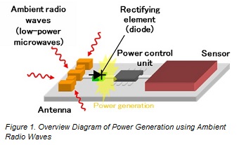
In preparation for the commencement of the true IoT era, energy harvesting technologies, which transform the minute sources of energy in the surrounding environment into electricity, have come under the spotlight in recent years as means for creating sensor networks that function without batteries. One such example reuses as electricity the low-power radio waves (microwaves), ubiquitous in open space, that are emitted from mobile phone base stations, for use in communications. Equipment used in generating electricity from ambient radio waves consists of a radio wave power generating element, which includes an antenna for collecting radio waves and a rectifying element (diode) that rectifies the radio waves (figure 1).
The responsiveness (sensitivity) of a diode to microwaves largely depends on the steepness of rectification characteristics and on diode size (capacity). Generally, Schottky barrier diodes, which utilize the rectification occurring at the junction formed between a metal and a semiconductor, are used as the diodes for power conversion. Due to rectification characteristics becoming slow at extremely low voltages and the size of elements being larger than several micrometers (μm), however, sensitivity to low-power microwaves weaker than microwatts (μW) was insufficient, and it was difficult to convert ambient radio waves into electricity. This led to a demand for diodes with increased sensitivity.
Page 1 of 2
Share on:


Suggested Items
Koh Young Showcases Award-winning Inspection Solutions at SMTconnect with SmartRep in Hall 4A.225
04/25/2024 | Koh Young TechnologyKoh Young Technology, the industry leader in True 3D measurement-based inspection solutions, will showcase an array of award-winning inspection and measurement solutions at SMTconnect alongside its sales partner, SmartRep, in booth 4A.225 at NürnbergMesse from June 11-13, 2023. The following offers a glimpse into what Koh Young will present at the tradeshow:
Real Time with… IPC APEX EXPO 2024: Plasmatreat: Innovative Surface Preparation Solutions
04/25/2024 | Real Time with...IPC APEX EXPOIn this interview, Editor Nolan Johnson speaks with Hardev Grewal, CEO and president of Plasmatreat, a developer of atmospheric plasma solutions. Plasmatreat uses clean compressed air and electricity to create plasma, offering environmentally friendly methods for surface preparation. Their technology measures plasma density for process optimization and can remove organic micro-contamination. Nolan and Hardev also discuss REDOX-Tool, a new technology for removing metal oxides.
Nanotechnology Market to Surpass $53.51 Billion by 2031
04/25/2024 | PRNewswireSkyQuest projects that the nanotechnology market will attain a value of USD 53.51 billion by 2031, with a CAGR of 36.4% over the forecast period (2024-2031).
Cadence, TSMC Collaborate on Wide-Ranging Innovations to Transform System and Semiconductor Design
04/25/2024 | Cadence Design SystemsCadence Design Systems, Inc. and TSMC have extended their longstanding collaboration by announcing a broad range of innovative technology advancements to accelerate design, including developments ranging from 3D-IC and advanced process nodes to design IP and photonics.
SMC Korea 2024 to Highlight Semiconductor Materials Trends and Innovations on Industry’s Path to $1 Trillion
04/24/2024 | SEMIWith Korea a major consumer of semiconductor materials and advanced materials a key driver of innovation on the industry’s path to $1 trillion, industry leaders and experts will gather at SMC (Strategic Materials Conference) Korea 2024 on May 29 at the Suwon Convention Center in Gyeonggi-do, South Korea to provide insights into the latest materials developments and trends. Registration is open.