


 The Government Circuit: Driving Resiliency and Economic Security on Both Sides of the Atlantic
 American Made Advocacy: Taking the Fight to Capitol Hill
 Defense Speak Interpreted: SWaPing Nanosatellites for Defense Systems
Laser Processing Method to Increase Efficiency of Optoelectronic Devices
April 15, 2019 | NRLEstimated reading time: 2 minutes
Scientists at the U.S. Naval Research Laboratory (NRL) discovered a new method to passivate defects in next generation optical materials to improve optical quality and enable the miniaturization of light emitting diodes and other optical elements.
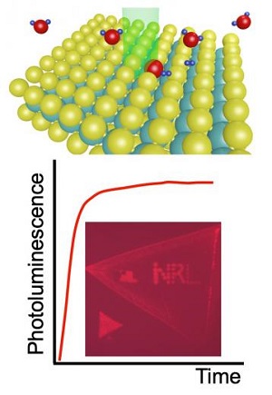
Image Caption: (Top) Illustration of a water molecule bonding at a sulfur vacancy in the MoS2 upon laser light exposure. (Bottom) Photoluminescence (PL) increase observed during laser light exposure in ambient. (Inset) Fluorescence image showing brightened regions spelling out “NRL.” (U.S. Naval Research Laboratory)
“From a chemistry standpoint, we have discovered a new photocatalytic reaction using laser light and water molecules, which is new and exciting,” said Saujan Sivaram, Ph.D., lead author of the study. “From a general perspective, this work enables the integration of high quality, optically active, atomically thin material in a variety of applications, such as electronics, electro-catalysts, memory, and quantum computing applications.”
The NRL scientists developed a versatile laser processing technique to significantly improve the optical properties of monolayer molybdenum disulphide (MoS2)—a direct gap semiconductor—with high spatial resolution. Their process produces a 100-fold increase in the material’s optical emission efficiency in the areas “written” with the laser beam.
According to Sivaram, atomically thin layers of transition metal dichalcogenides (TMDs), such as MoS2, are promising components for flexible devices, solar cells, and optoelectronic sensors due to their high optical absorption and direct band gap.
“These semiconducting materials are particularly advantageous in applications where weight and flexibility are a premium,” he said. “Unfortunately, their optical properties are often highly variable and non-uniform making it critical to improve and control the optical properties of these TMD materials to realize reliable high efficiency devices.”
“Defects are often detrimental to the ability of these monolayer semiconductors to emit light,” Sivaram said. “These defects act as non-radiative trap states, producing heat instead of light, therefore, removing or passivating these defects is an important step towards high efficiency optoelectronic devices.”
In a traditional LED, approximately 90% of the device is a heat sink to improve cooling. Reduced defects enable smaller devices to consume less power, which results in a longer operational lifetime for distributed sensors and low-power electronics.
The researchers demonstrated that water molecules passivate the MoS2 only when exposed to laser light with an energy above the band gap of the TMD. The result is an increase in photoluminescence with no spectral shift.
Treated regions maintain a strong light emission compared to the untreated regions that exhibit much a weaker emission. This suggest that the laser light drives a chemical reaction between the ambient gas molecules and the MoS2.
“This is a remarkable achievement,” said Berend Jonker, Ph.D., senior scientist and principal investigator. “The results of this study pave the way for the use of TMD materials critical to the success of optoelectronic devices and relevant to the Department of Defense mission.”
Share on:


Suggested Items
Real Time with... IPC APEX EXPO 2024: Sustainability in the Industry
04/26/2024 | Real Time with...IPC APEX EXPOGuest Editor Henry Crandall and Chris Nash of Indium Corporation discuss the company's 90th anniversary and its focus on sustainability. They focus on the benefits of sustainable materials, their compatibility, and value propositions. The conversation also highlights how Durafuse LT technology's role in reducing reflow temperatures is leading to significant cost and energy savings. Nash also touches on downstream sustainability efforts such as using recycled materials for packaging.
SMC Korea 2024 to Highlight Semiconductor Materials Trends and Innovations on Industry’s Path to $1 Trillion
04/24/2024 | SEMIWith Korea a major consumer of semiconductor materials and advanced materials a key driver of innovation on the industry’s path to $1 trillion, industry leaders and experts will gather at SMC (Strategic Materials Conference) Korea 2024 on May 29 at the Suwon Convention Center in Gyeonggi-do, South Korea to provide insights into the latest materials developments and trends. Registration is open.
Groundbreaking Ceremony Marks the Beginning of a New Era for Newccess Industrial; The Construction of the MINGXIN Building
04/12/2024 | Newccess IndustrialOn a clear and sunny day in March, the groundbreaking ceremony for the MINGXIN Building took place in Shenzhen, China. This moment marked the official commencement of construction for a project that will reshape the semiconductor materials industry.
The Need for a Holistic Global Sustainability Standard
04/10/2024 | Michael Ford, Aegis SoftwareNo one can deny that the resources of our fragile planet are finite. The environment seems like a third party, subject to constant degradation. We’re acutely aware of the effects of pollution on our climate, and despite our “throw-away” culture, recycling and recovery of materials has remained relatively expensive, even as we use more energy just to survive.
iNEMI Publishes Four Roadmap Topics
04/04/2024 | iNEMIThe International Electronics Manufacturing Initiative (iNEMI) announces the availability of the first roadmap topics in the new iNEMI Roadmap format. Printed circuit boards, sustainable electronics, smart manufacturing, and mmWave materials and test are now available online.