


 The Government Circuit: Driving Resiliency and Economic Security on Both Sides of the Atlantic
 American Made Advocacy: Taking the Fight to Capitol Hill
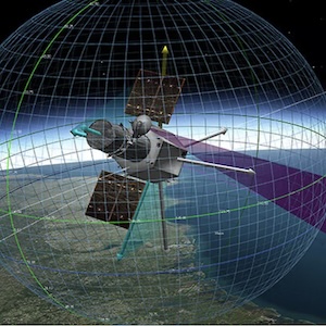
 Defense Speak Interpreted: SWaPing Nanosatellites for Defense Systems
KAIST Perfectly Transfers Nanowires onto a Flexible Substrate
September 17, 2018 | KAISTEstimated reading time: 2 minutes
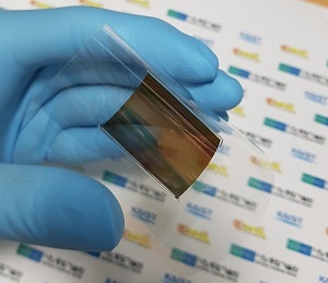
Boasting excellent physical and chemical properties, nanowires (NWs) are suitable for fabricating flexible electronics; therefore, technology to transfer well-aligned wires plays a crucial role in enhancing performance of the devices. A KAIST research team succeeded in developing NW-transfer technology that is expected to enhance the existing chemical reaction-based NW fabrication technology that has this far showed low performance in applicability and productivity.
Figure 1: Photograph of the fabricated wafer-scale fully aligned and ultralong Au nanowire array on a flexible substrate
NWs, one of the most well-known nanomaterials, have the structural advantage of being small and lightweight. Hence, NW-transfer technology has drawn attention because it can fabricate high-performance, flexible nanodevices with high simplicity and throughput.
A conventional nanowire-fabrication method generally has an irregularity issue since it mixes chemically synthesized nanowires in a solution and randomly distributes the NWs onto flexible substrates. Hence, numerous nanofabrication processes have emerged, and one of them is master-mold-based, which enables the fabrication of highly ordered NW arrays embedded onto substrates in a simple and cost-effective manner, but its employment is limited to only some materials because of its chemistry-based NW-transfer mechanism, which is complex and time consuming. For the successful transfer, it requires that adequate chemicals controlling the chemical interfacial adhesion between the master mold, NWs, and flexible substrate be present.
This method involves sequentially forming a nanosacrificial layer and NWs on a nanograting substrate that becomes the master mold for the transfer, then weakening the structure of the nanosacrificial layer through a dry etching process. The nanosacrificial layer very weakly holds the nanowires on the master mold. Therefore, when using a flexible substrate material, the nanowires are very easily transferred from the master mold to the substrate, just like a piece of tape lifting dust off a carpet.
This technology uses common physical vapor deposition and does not rely on NW materials, making it easy to fabricate NWs onto the flexible substrates.
Using this technology, the team was able to fabricate a variety of metal and metal-oxide NWs, including gold, platinum, and copper – all perfectly aligned on a flexible substrate. They also confirmed that it can be applied to creating stable and applicable devices in everyday life by successfully applying it to flexible heaters and gas sensors.
PhD Min-Ho Seo who led this research said, “We have successfully aligned various metals and semiconductor NWs with excellent physical properties onto flexible substrates and applied them to fabricated devices. As a platform-technology, it will contribute to developing high-performing and stable electronic devices.”
Share on:


Suggested Items
Insulectro’s 'Storekeepers' Extend Their Welcome to Technology Village at IPC APEX EXPO
04/03/2024 | InsulectroInsulectro, the largest distributor of materials for use in the manufacture of PCBs and printed electronics, welcomes attendees to its TECHNOLOGY VILLAGE during this year’s IPC APEX EXPO at the Anaheim Convention Center, April 9-11, 2024.
ENNOVI Introduces a New Flexible Circuit Production Process for Low Voltage Connectivity in EV Battery Cell Contacting Systems
04/03/2024 | PRNewswireENNOVI, a mobility electrification solutions partner, introduces a more advanced and sustainable way of producing flexible circuits for low voltage signals in electric vehicle (EV) battery cell contacting systems.
Heavy Copper PCBs: Bridging the Gap Between Design and Fabrication, Part 1
04/01/2024 | Yash Sutariya, Saturn Electronics ServicesThey call me Sparky. This is due to my talent for getting shocked by a variety of voltages and because I cannot seem to keep my hands out of power control cabinets. While I do not have the time to throw the knife switch to the off position, that doesn’t stop me from sticking screwdrivers into the fuse boxes. In all honesty, I’m lucky to be alive. Fortunately, I also have a talent for building high-voltage heavy copper circuit boards. Since this is where I spend most of my time, I can guide you through some potential design for manufacturability (DFM) hazards you may encounter with heavy copper design.
Trouble in Your Tank: Supporting IC Substrates and Advanced Packaging, Part 5
03/19/2024 | Michael Carano -- Column: Trouble in Your TankDirect metallization systems based on conductive graphite or carbon dispersion are quickly gaining acceptance worldwide. Indeed, the environmental and productivity gains one can achieve with these processes are outstanding. In today’s highly competitive and litigious environment, direct metallization reduces costs associated with compliance, waste treatment, and legal issues related to chemical exposure. What makes these processes leaders in the direct metallization space?
AT&S Shines with Purest Copper on World Recycling Day
03/18/2024 | AT&SThe Styrian microelectronics specialist AT&S is taking World Recycling Day as an opportunity to review the progress that has been made in recent months at its sites around the world in terms of the efficient use of resources:
Copyright © 2024 I-Connect007 | IPC Publishing Group Inc. All rights reserved.
Log in