


 The Government Circuit: Driving Resiliency and Economic Security on Both Sides of the Atlantic
 American Made Advocacy: Taking the Fight to Capitol Hill
 Defense Speak Interpreted: SWaPing Nanosatellites for Defense Systems
Miniaturizing the Brain of a Drone
July 12, 2017 | MITEstimated reading time: 6 minutes
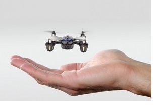
In recent years, engineers have worked to shrink drone technology, building flying prototypes that are the size of a bumblebee and loaded with even tinier sensors and cameras. Thus far, they have managed to miniaturize almost every part of a drone, except for the brains of the entire operation — the computer chip.
Standard computer chips for quadcoptors and other similarly sized drones process an enormous amount of streaming data from cameras and sensors, and interpret that data on the fly to autonomously direct a drone’s pitch, speed, and trajectory. To do so, these computers use between 10 and 30 watts of power, supplied by batteries that would weigh down a much smaller, bee-sized drone.
Now, engineers at MIT have taken a first step in designing a computer chip that uses a fraction of the power of larger drone computers and is tailored for a drone as small as a bottlecap. They will present a new methodology and design, which they call “Navion,” at the Robotics: Science and Systems conference, held this week at MIT.
The team, led by Sertac Karaman, the Class of 1948 Career Development Associate Professor of Aeronautics and Astronautics at MIT, and Vivienne Sze, an associate professor in MIT's Department of Electrical Engineering and Computer Science, developed a low-power algorithm, in tandem with pared-down hardware, to create a specialized computer chip.
The key contribution of their work is a new approach for designing the chip hardware and the algorithms that run on the chip. “Traditionally, an algorithm is designed, and you throw it over to a hardware person to figure out how to map the algorithm to hardware,” Sze says. “But we found by designing the hardware and algorithms together, we can achieve more substantial power savings.”
“We are finding that this new approach to programming robots, which involves thinking about hardware and algorithms jointly, is key to scaling them down,” Karaman says.
The new chip processes streaming images at 20 frames per second and automatically carries out commands to adjust a drone’s orientation in space. The streamlined chip performs all these computations while using just below 2 watts of power — making it an order of magnitude more efficient than current drone-embedded chips.
Karaman, says the team’s design is the first step toward engineering “the smallest intelligent drone that can fly on its own.” He ultimately envisions disaster-response and search-and-rescue missions in which insect-sized drones flit in and out of tight spaces to examine a collapsed structure or look for trapped individuals. Karaman also foresees novel uses in consumer electronics.
“Imagine buying a bottlecap-sized drone that can integrate with your phone, and you can take it out and fit it in your palm,” he says. “If you lift your hand up a little, it would sense that, and start to fly around and film you. Then you open your hand again and it would land on your palm, and you could upload that video to your phone and share it with others.”
Karaman and Sze’s co-authors are graduate students Zhengdong Zhang and Amr Suleiman, and research scientist Luca Carlone.
From the ground up
Current minidrone prototypes are small enough to fit on a person’s fingertip and are extremely light, requiring only 1 watt of power to lift off from the ground. Their accompanying cameras and sensors use up an additional half a watt to operate.
“The missing piece is the computers — we can’t fit them in terms of size and power,” Karaman says. “We need to miniaturize the computers and make them low power.”
The group quickly realized that conventional chip design techniques would likely not produce a chip that was small enough and provided the required processing power to intelligently fly a small autonomous drone.
“As transistors have gotten smaller, there have been improvements in efficiency and speed, but that’s slowing down, and now we have to come up with specialized hardware to get improvements in efficiency,” Sze says.
The researchers decided to build a specialized chip from the ground up, developing algorithms to process data, and hardware to carry out that data-processing, in tandem.
Tweaking a formula
Specifically, the researchers made slight changes to an existing algorithm commonly used to determine a drone’s “ego-motion,” or awareness of its position in space. They then implemented various versions of the algorithm on a field-programmable gate array (FPGA), a very simple programmable chip. To formalize this process, they developed a method called iterative splitting co-design that could strike the right balance of achieving accuracy while reducing the power consumption and the number of gates.
A typical FPGA consists of hundreds of thousands of disconnected gates, which researchers can connect in desired patterns to create specialized computing elements. Reducing the number gates with co-design allowed the team to chose an FPGA chip with fewer gates, leading to substantial power savings.
“If we don’t need a certain logic or memory process, we don’t use them, and that saves a lot of power,” Karaman explains.
Each time the researchers tweaked the ego-motion algorithm, they mapped the version onto the FPGA’s gates and connected the chip to a circuit board. They then fed the chip data from a standard drone dataset — an accumulation of streaming images and accelerometer measurements from previous drone-flying experiments that had been carried out by others and made available to the robotics community.
“These experiments are also done in a motion-capture room, so you know exactly where the drone is, and we use all this information after the fact,” Karaman says.
Memory savings
For each version of the algorithm that was implemented on the FPGA chip, the researchers observed the amount of power that the chip consumed as it processed the incoming data and estimated its resulting position in space.
The team’s most efficient design processed images at 20 frames per second and accurately estimated the drone’s orientation in space, while consuming less than 2 watts of power.
The power savings came partly from modifications to the amount of memory stored in the chip. Sze and her colleagues found that they were able to shrink the amount of data that the algorithm needed to process, while still achieving the same outcome. As a result, the chip itself was able to store less data and consume less power.
“Memory is really expensive in terms of power,” Sze says. “Since we do on-the-fly computing, as soon as we receive any data on the chip, we try to do as much processing as possible so we can throw it out right away, which enables us to keep a very small amount of memory on the chip without accessing off-chip memory, which is much more expensive.”
In this way, the team was able to reduce the chip’s memory storage to 2 megabytes without using off-chip memory, compared to a typical embedded computer chip for drones, which uses off-chip memory on the order of a few gigabytes.
“Any which way you can reduce the power so you can reduce battery size or extend battery life, the better,” Sze says.
This summer, the team will mount the FPGA chip onto a drone to test its performance in flight. Ultimately, the team plans to implement the optimized algorithm on an application-specific integrated circuit, or ASIC, a more specialized hardware platform that allows engineers to design specific types of gates, directly onto the chip.
“We think we can get this down to just a few hundred milliwatts,” Karaman says. “With this platform, we can do all kinds of optimizations, which allows tremendous power savings.”
This research was supported, in part, by Air Force Office of Scientific Research and the National Science Foundation.
Share on:


Suggested Items
iNEMI Packaging Tech Topic Series: Role of EDA in Advanced Semiconductor Packaging
04/26/2024 | iNEMIAdvanced semiconductor packaging with heterogenous integration has made on-package integration of multiple chips a crucial part of finding alternatives to transistor scaling. Historically, EDA tools for front-end and back-end design have evolved separately; however, design complexity and the increased number of die-to-die or die-to-substrate interconnections has led to the need for EDA tools that can support integration of overall design planning, implementation, and system analysis in a single cockpit.
Cadence, TSMC Collaborate on Wide-Ranging Innovations to Transform System and Semiconductor Design
04/25/2024 | Cadence Design SystemsCadence Design Systems, Inc. and TSMC have extended their longstanding collaboration by announcing a broad range of innovative technology advancements to accelerate design, including developments ranging from 3D-IC and advanced process nodes to design IP and photonics.
Ansys, TSMC Enable a Multiphysics Platform for Optics and Photonics, Addressing Needs of AI, HPC Silicon Systems
04/25/2024 | PRNewswireAnsys announced a collaboration with TSMC on multiphysics software for TSMC's Compact Universal Photonic Engines (COUPE). COUPE is a cutting-edge Silicon Photonics (SiPh) integration system and Co-Packaged Optics platform that mitigates coupling loss while significantly accelerating chip-to-chip and machine-to-machine communication.
Siemens’ Breakthrough Veloce CS Transforms Emulation and Prototyping with Three Novel Products
04/24/2024 | Siemens Digital Industries SoftwareSiemens Digital Industries Software launched the Veloce™ CS hardware-assisted verification and validation system. In a first for the EDA (Electronic Design Automation) industry, Veloce CS incorporates hardware emulation, enterprise prototyping and software prototyping and is built on two highly advanced integrated circuits (ICs) – Siemens’ new, purpose-built Crystal accelerator chip for emulation and the AMD Versal™ Premium VP1902 FPGA adaptive SoC (System-on-a-chip) for enterprise and software prototyping.
Listen Up! The Intricacies of PCB Drilling Detailed in New Podcast Episode
04/25/2024 | I-Connect007In episode 5 of the podcast series, On the Line With: Designing for Reality, Nolan Johnson and Matt Stevenson continue down the manufacturing process, this time focusing on the post-lamination drilling process for PCBs. Matt and Nolan delve into the intricacies of the PCB drilling process, highlighting the importance of hole quality, drill parameters, and design optimization to ensure smooth manufacturing. The conversation covers topics such as drill bit sizes, aspect ratios, vias, challenges in drilling, and ways to enhance efficiency in the drilling department.