


 The Chemical Connection: Reducing Etch System Water Usage, Part 2
 It’s Only Common Sense: Nice Guys Really Can Finish First
 The Right Approach: I Hear the Train A Comin'
Ansys Multiphysics Solutions Enable Signoff Verification for Intel 16 Process Node
July 11, 2023 | PRNewswireEstimated reading time: 1 minute
Intel Foundry Services (IFS) certified Ansys multiphysics solutions for signoff verification of advanced integrated circuits (ICs) designed with the Intel 16 silicon manufacturing process. The predictive accuracy of Ansys' power integrity and signal integrity platforms helps designers increase the performance of edge AI, graphic processing, and wireless communication products by avoiding wasteful over-design. The collaboration with IFS validated a seamless electronic design automation (EDA) flow that delivers high productivity for joint customers.
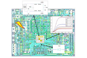
Ansys Redhawk-SC, Ansys Totem, and Ansys PathFinder-SC (pictured) support power integrity, signal integrity, and reliability signoff requirements for the Intel 16 process node
Ansys RedHawk-SC and Ansys Totem are recognized as industry standards for power integrity signoff of digital and analog designs. The solutions' cloud-enabled data infrastructure provides unparalleled capacity to analyze full-chip designs, hierarchically or flat. Ansys PathFinder-SC uses the same elastic compute infrastructure to verify the electrostatic discharge (ESD) protection circuitry found on all chips.
"Ansys and IFS, with a history of close collaboration, are pleased with the broad support of our Intel 16 process including our RF capabilities," said Rahul Goyal, vice president & general manager for Intel's Product & Design Ecosystem Enablement group. "We believe in providing our foundry customers with the widest possible array of industry-leading EDA tools that work in their existing design platforms and that make optimal use of our advanced manufacturing technology."
"Ansys works with leading foundry partners like Intel Foundry Services to address complex multiphysics challenges and meet stringent power, performance, and reliability requirements," said John Lee, vice president and general manager of the electronics, semiconductor, and optics business unit at Ansys. "Ansys' signoff platform helps empower mutual customers to accelerate design convergence with greater confidence thanks to the collaborative work between the companies to ensure silicon predictive accuracy and a smooth user experience."
Share on:


Suggested Items
Real Time with… IPC APEX EXPO 2024: My Role as a Technology Solutions Director
05/02/2024 | Real Time with...IPC APEX EXPOPeter Tranitz, senior director of technology solutions at IPC, shares insights into his role as the design initiative lead. He details his advocacy work, industry support, and the responsibilities of the design initiative committee. The conversation also covers the revamping of standards, the IPC Design Competition, and the implementation of design rules in software tools.
Real Time with… IPC APEX EXPO 2024: Ventec Discusses New Pro-bond Family of Advanced Products
05/01/2024 | Real Time with...IPC APEX EXPOChris Hanson, Ventec's Global Head of IMS Technology, outlines the launch of four pro-bond formulas that deliver an outstanding combination of low dissipation factor (Df) with a dielectric constant (Dk) range to maximize the design window for critical PCB parameters. As Chris points out, Pro-bond is designed for low-loss, high-speed applications, while thermal-bond dissipates heat from a component through the board to a heat sink.
IPC's Vision for Empowering PCB Design Engineers
04/30/2024 | Robert Erickson, IPCAs architects of innovation, printed circuit board designers are tasked with translating increasingly complex concepts into tangible designs that power our modern world. IPC provides the necessary community, standards framework, and education to prepare these pioneers as they explore the boundaries of what’s possible, equipping engineers with the knowledge, skills, and resources required to thrive in an increasingly dynamic field.
On the Line With… Talks With Cadence Expert on SI/PI for PCB Designers
05/02/2024 | I-Connect007In “PCB 3.0: A New Design Methodology—SI/PI for PCB Designers,” subject matter expert Brad Griffin, Cadence Design Systems, discusses how an intelligent system design methodology can move some signal and power integrity decision-making into the physical design space, offering real-time feedback.
iNEMI Packaging Tech Topic Series: Role of EDA in Advanced Semiconductor Packaging
04/26/2024 | iNEMIAdvanced semiconductor packaging with heterogenous integration has made on-package integration of multiple chips a crucial part of finding alternatives to transistor scaling. Historically, EDA tools for front-end and back-end design have evolved separately; however, design complexity and the increased number of die-to-die or die-to-substrate interconnections has led to the need for EDA tools that can support integration of overall design planning, implementation, and system analysis in a single cockpit.