


 The Government Circuit: Driving Resiliency and Economic Security on Both Sides of the Atlantic
 American Made Advocacy: Taking the Fight to Capitol Hill
 Defense Speak Interpreted: SWaPing Nanosatellites for Defense Systems
Terahertz Technology Escapes the Cold
July 10, 2019 | ETH ZurichEstimated reading time: 5 minutes
Terahertz (THz) radiation is a bit like a treasure chest that resists being opened fully. Residing in the electromagnetic spectrum between the infrared and microwave regions, THz radiation combines a range of properties that are ideal with a view to applications. It provides a window to unique spectroscopic information about molecules and solids, it can penetrate non-conducting materials such as textiles and biological tissue, and it does so without ionising—and hence damaging—the object, or subject, under study. This opens up intriguing prospects for non-invasive imaging and non-destructive quality control, among other applications. But whereas there is no shortage in ideas for potential uses, their implementation is hampered by a lack of practical technologies for generating and detecting THz radiation.
Therefore the excitement as Lorenzo Bosco, Martin Franckié and colleagues from the group of Jérôme Faist at the Institute for Quantum Electronics of ETH Zurich reported now the realization of a THz quantum cascade laser that operates at a temperature of 210 K (-63 °C). That is the highest operational temperature achieved so far for this type of device. More importantly, this is the first time that operation of such a device has been demonstrated in a temperature regime where no cryogenic coolants are needed. Instead, Bosco et al. used a thermoelectric cooler, which is much more compact, cheaper and easier to maintain than cryogenic equipment. With this advance, they removed the main obstacles on the route to various practical applications.
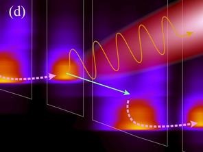
a) The thermoelectrically cooled laser box with the laser mounted on top of a Peltier element (white square), allowing operation between 195 K and 210.5 K with the laser emitting vertically through the window in the top lid. b) The laser chip as mounted in the laser box, contacted with thin gold wires bonded on top of several laser ridges. c) Schematic of one laser ridge; the horizontal lines show the quantum-well structure formed by layered semiconductors. The ridge (150 micrometres wide) is sandwiched between thin layers of copper. d) Conduction band edge (white lines) tilted by the applied operation bias, with the electron density resolved in energy shown in colour. The electrical bias drives electrons through the non-radiative transitions indicated by the dashed arrow. This pumps the state in the thin well, which becomes more populated than the state in the wider well indicated by the green arrow, allowing for net stimulated emission of terahertz photons.
A Cascade Towards Applications
Quantum cascade lasers (QCLs) have long been established as a natural concept for THz devices. Like many lasers that are widely used as sources of light in the visible-to-infrared frequency region, QCLs are based on semiconductor materials. But compared to typical semiconductor lasers used, for instance, in barcode readers or laser pointers, QCLs operate according to a fundamentally different concept to achieve light emission. In short, they are built around repeated stacks of precisely engineered semiconductor structures (see the figure, panel c), which are designed such that suitable electronic transitions take place in them (panel d). QCLs have been proposed in 1971, but they were first demonstrated only in 1994, by Faist and colleagues, then working at Bell Laboratories (US). The approach has proved its value in a board range of experiments, both fundamental and applied, mainly in the infrared region. The development of QCLs for THz emission has made substantial advances, too, starting from 2001. Widespread use has been hindered though by the requirement for cryogenic coolants -- typically liquid helium -- which adds substantial complexity and cost, and makes devices large and less mobile. Progress towards operation of THz QCLs at higher temperatures got essentially stuck seven years ago, when operation of devices at around 200 K (-73 °C) was achieved.
Page 1 of 2
Share on:


Suggested Items
DuPont Showcases AI Innovations Featuring Advanced Interconnects at 2024 International Electronic Circuits Exhibition
05/13/2024 | DuPontDuPont announced it will showcase its comprehensive range of advanced circuit materials and solutions at the 2024 International Electronic Circuits Exhibition in Shanghai. With a product portfolio that includes fine line, signal integrity, power and thermal management, DuPont will exhibit at Booth #8L06 at the National Exhibition and Convention Center (NECC) from May 13 to 15.
MKS’ Atotech to Participate in ECTC
05/10/2024 | MKS’ AtotechAt this year’s 74th IEEE Electronic Components and Technology Conference (ECTC), MKS’ Atotech will present and demonstrate its latest product and service innovations.
The Chemical Connection: Reducing Etch System Water Usage, Part 2
05/02/2024 | Don Ball -- Column: The Chemical ConnectionIn my last column, I reviewed some relatively simple ways to reduce water usage in existing etch systems: cutting down cooling coil water flow, adding chillers to replace plant water for cooling, lowering flow rate nozzles for rinses, etc. This month, I’ll continue with more ways to control water usage in your etcher. Most of these are not easily retrofittable to existing equipment but should be given serious consideration when new equipment is contemplated. With the right combination of add-ons, it is possible to bring the amount of water used in an etch system to almost zero.
Designer’s Notebook: What Designers Need to Know About Manufacturing, Part 2
04/24/2024 | Vern Solberg -- Column: Designer's NotebookThe printed circuit board (PCB) is the primary base element for providing the interconnect platform for mounting and electrically joining electronic components. When assessing PCB design complexity, first consider the component area and board area ratio. If the surface area for the component interface is restricted, it may justify adopting multilayer or multilayer sequential buildup (SBU) PCB fabrication to enable a more efficient sub-surface circuit interconnect.
Insulectro’s 'Storekeepers' Extend Their Welcome to Technology Village at IPC APEX EXPO
04/03/2024 | InsulectroInsulectro, the largest distributor of materials for use in the manufacture of PCBs and printed electronics, welcomes attendees to its TECHNOLOGY VILLAGE during this year’s IPC APEX EXPO at the Anaheim Convention Center, April 9-11, 2024.